
1. Introduction
Classical electronic processors have been scaled by Moore’s law, but capacity growth is now limited due to thermal limits, quantum tunneling, and RC delays. The optical cubic propagation architecture I am working on aims to overcome these limits through photon flux and volumetric parallelism.
2. Electronics vs Optics Comparison
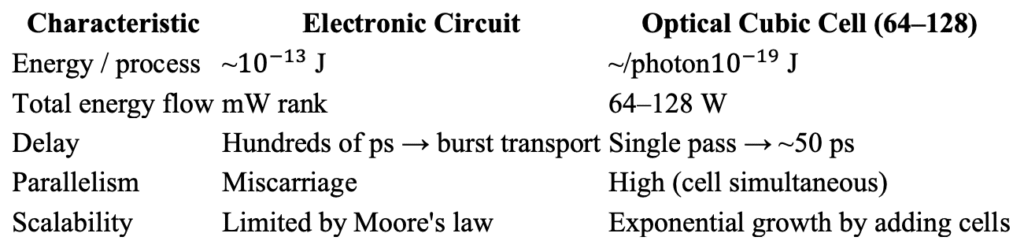
3. Scaling Analysis
- 64 cells: 1.61 × 10²⁰ photon/s, 64 W
- 128 cells: 3.23 × 10²⁰ photon/s, 128 W
- 256 cells: 6.46 × 10²⁰ photon/s, 256 W
- 512 cells: 1.29 × 10²¹ photon/s, 512 W
As the number of cells increases, the processing capacity grows volumetrically, not linearly.
4. Wavelength Effect
- 700 nm (red): 1.77 eV → lower energy, safer.
- 500 nm (green): 2.48 eV → Optimal balance
- 250 nm (UV): 4.96 eV → high energy, chemical bond-breaking potential.
As the wavelength decreases, the photon energy increases, the processing capacity increases, but the material strength becomes critical.
5. Hybrid Architecture
- Optical processing layer: Speed and parallelism.
- Electronic memory layer: Data storage and addressing.
- Interface: Photon–electron conversion with photodiodes and resonators.
- Control module: Phase lock and synchronization.
This hybrid structure provides a combination of optical speed + electronic memory security.
6. Potential Applications
- Defense: Real-time signal processing, radar/sonar data density.
- Medicine: Optical tomography and biosignal analysis.
- Energy: Data processing in photovoltaic systems.
- Industry: Big data analytics, artificial intelligence accelerators.
7. Challenges
- Phase stability and intercellular synchronization.
- Wafer-level production costs.
- Optical memory integration.
- Lack of standard design tools.
8. Conclusion
Optical cubic processing architecture transforms computer capacities into systems that process information at exponential density, near the speed of light . Beyond electronic limits, hybrid architecture combines with optical speed + electronic memory security to form the next generation computing paradigm.
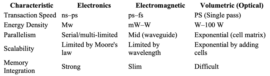
Electronics – Electromagnetics – Volumetric Architecture Comparison
1. Introduction
Information processing technologies have developed with three main paradigms:
- Electronic architecture: Transistor and CMOS-based processors.
- Electromagnetic architecture: Microwave, RF, and waveguide-based systems.
- Volumetric (optical/photonic) architecture: Exponential parallelism with photon flux and cubic cells.
Each architecture has different advantages and limits. This report compares the volumetric propagation paradigm you are working on with classical electronic and electromagnetic systems.
2. Electronic Architecture
- Basic principle: Electron flow creates logic gates with transistors.
- Advantages:
- Mature manufacturing technology (CMOS).
- High integration (billions of transistors).
- Reliable memory and addressing.
- Limitations:
- RC delay → speed limit.
- Energy efficiency decreases → thermal losses.
- Quantum tunneling → problem in sub-5nm production.
3. Electromagnetic Architecture
- Basic principle: Information processing with RF/microwave waves.
- Advantages:
- High frequency (GHz–THz range).
- Low loss with waveguides.
- Critical role in wireless communication.
- Limitations:
- Integration challenge → large wavelength.
- Energy density is limited.
- Efficiency is low at the logic gate level.
4. Volumetric (Optical/Photonic) Architecture
- Basic principle: Photon flow, parallel processing in cubic cells.
- Advantages:
- Near-lightning speed operation.
- Exponential parallelism as the number of cells increases.
- Photon energy can be controlled by wavelength selection.
- Limitations:
- Phase stability is critical.
- Memory integration is challenging.
- Wafer production costs are high.
5. Comparative Table
6. Application Areas
- Electronics: General-purpose processors, memory, mobile devices.
- Electromagnetic: Communication , radar, RF sensors.
- Volumetric: Supercomputers, artificial intelligence accelerators, medical imaging, defense systems.
7. Future Perspective
- Electronics: 3D stacking and quantum-powered hybrid solutions.
- Electromagnetic: New communication protocols in the terahertz band.
- Volumetric: The new paradigm → optical processors + electronic memory hybrid architecture.
8. Conclusion
- The electronic architecture is mature and reliable, but it has reached the speed/energy limit.
- Electromagnetic architecture is strong in communication, but its processing intensity is limited.
- Volumetric architecture represents the computer paradigm of the future with its exponential processing capacity.
Mathematics and Physics Foundations of Volumetric Architecture
1. Introduction
Volumetric architecture, unlike classical electronic and planar electromagnetic systems, is based on three-dimensional photon flux and volumetric parallelism. In this approach, information processing is defined by Maxwell’s equations, wave mechanics, and quantum photonics principles.
2. Mathematical Foundations
2.1 Maxwell’s Equations
At the core of volumetric architecture are electromagnetic wave equations:
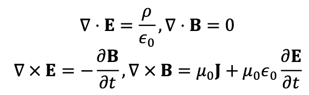
- Electronics: Solved through current and voltage.
- Optical volumetric: Solved through wave vector () and phase relationships.𝐤
2.2 Wave Equation
Light propagation in optical cells is described by the wave equation:
- Solution: 𝐄(𝑟, 𝑡) = 𝐸0𝑒i(𝐤⋅r-wt )
- Parallel processing → intercellular phase pairing.
2.3 Photon Energy
The energy of each photon is:
𝐸 = ℎ ⋅ 𝑓 = ℎ ⋅ 𝑐 / 𝜆
- 700 nm → 1.77 eV
- 500 nm → 2.48 eV
- 250 nm → 4.96 eV
As the wavelength becomes shorter, the processing capacity increases.
2.4 Volumetric Parallelism
Total processing capacity when the number of cells is:𝑁
𝐶(𝑁) = 𝑁 ⋅ 𝑃 / 𝐸
Here:
- 𝑃 : Power per cell (W)
- 𝐸 : Single photon energy (J)
The capacity is linear with the number of cells, but provides exponential density due to volumetric spread.
3. Physical Foundations
3.1 Phase Matching
- Optical pathway difference between cells. Δ𝜙 = 𝑚 ⋅ 2𝜋.
- If phase lock is not provided, the operation is incorrect.
3.2 Optical Logic Gates
- AND: Superposition of two light waves.
- OR: Any input is sufficient in wave interference.
- NOT: It is provided by phase reversal.
3.3 Energy Density
- Electronics: Capacitive charge/discharge → mW.
- Optics: Photon flux → W–100 W.
- This difference determines the processing intensity of the volumetric architecture.
4. Mathematical Modeling
4.1 Cubic Cell Matrix
For each cell:
𝐼cell = 𝑃 / 𝐸
Sum:
𝐼total = 𝑁 ⋅ 𝐼cell
4.2 Exponential Spread
Information processing in volumetric architecture:
𝐼vol ∝ 𝑁3
Exponential processing capacity → 3D cubic spread.
5. Application Scenarios
- Defense: Volumetric processing of radar/sonar data.
- Medicine: Optical tomography, biosignal analysis.
- Energy: Data processing in photovoltaic systems.
- Industry: AI accelerators, big data analytics.
6. Conclusion
Mathematical and physics foundations of volumetric architecture:
- Wave propagation by Maxwell’s equations,
- Processing capacity with photon energy,
- Accuracy with phase matching ,
- Exponential density with cubic parallelism.
This paradigm transcends the limitations of classical electronic and electromagnetic systems, providing near-lightning-fast, exponential processing capability.
Visualization Segments
1. Number of Cells → Processing Capacity Curve
- X-axis: Number of cells (64, 128, 256, 512)
- Y-axis: Processing capacity (photons/s)
- The curve shows linear increase:
- 64 cells → 1.61 × 10²⁰ photons/s
- 128 cells → 3.23 × 10²⁰ photons/s
- 256 cells → 6.46 × 10²⁰ photons/s
- 512 cells → 1.29 × 10²¹ photons/s
2. Graph of Wavelength → Photon Energy
- X-axis: Wavelength (nm)
- Y-axis: Photon energy (eV)
- Points:
- 700 nm → 1.77 eV
- 500 nm → 2.48 eV
- 250 nm → 4.96 eV
As the wavelength decreases, the photon energy increases, the processing capacity of the system increases, but the material strength becomes critical.
Comment
Together, these two graphs reveal that:
- As the number of cells increases, the processing capacity grows linearly, but exponential density is achieved thanks to volumetric spread.
- As the wavelength shortens, the photon energy increases, → the system becomes more powerful, but phase stability and material boundaries are more critical.
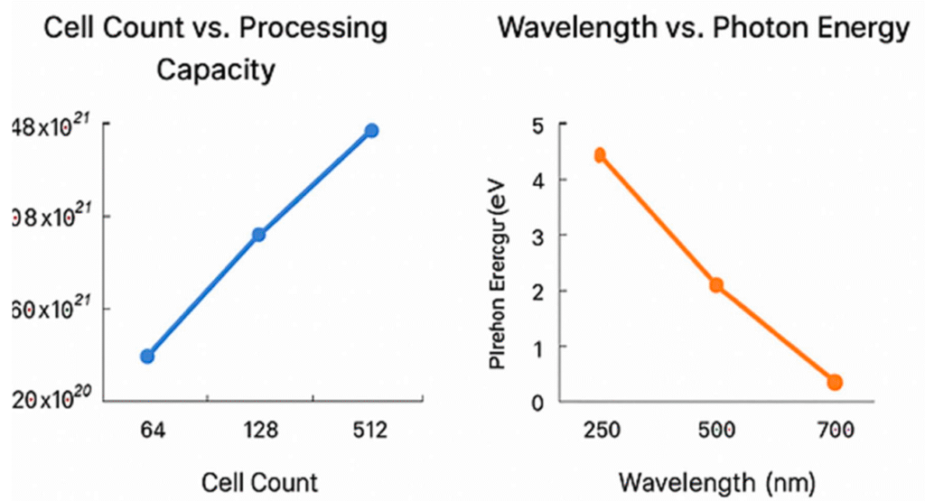
As the number of cells increases, the processing capacity increases linearly, and as the wavelength decreases, the photon energy increases. When these two effects are combined, the exponential processing density of the system emerges.
- Left graph: Processing capacity (photon/s) curve as the number of cells increases.
- Right graph: Photon energy (eV) curve by wavelength.
Information : Structure of Photon
The photon is the quantum of the electromagnetic field: it is a massless, elementary particle with no electric charge and moving at the speed of light. It exhibits both wave and particle properties, which is why it has a special place in quantum mechanics.
Physical and Quantum Structure of the Photon
1. Key Features
- Mass: Its resting mass is zero (), but it has energy. (𝑚0 = 0)
- Electric charge: Non-existent → can carry electromagnetic interactions, but electrically neutral.
- Spin: It is in the 1 → boson class.
- Speed: Moves steadily and at maximum speed in space: .𝑐 = 299,792,458 m/s
- Life time: It is stable → non-degradable, stable.
2. Quantum Definition
The photon is produced by quantization of the electromagnetic field. Each photon is a packet of energy:
𝐸 = ℎ ⋅ 𝑓 = ℎ ⋅ 𝑐 / 𝜆
Here:
- 𝐸 : Photon energy
- ℎ : Planck’s constant (6.626 × 10⁻³ Js)
- 𝑓 : Frequency
- 𝜆 : Wavelength
As the wavelength gets shorter, the photon energy increases, → UV photons are more energetic, while IR photons are lower energy.
3. Wave-Particle Duality
- Like a wave: It shows interference, diffraction, polarization.
- Particle-like: The photoelectric effect provides energy transfer in phenomena such as Compton scattering.
4. Interactions
- It is the carrier of the electromagnetic force.
- By interacting with the energy levels of matter at the atomic level:
- Absorbable (absorption)
- Radiable (emission)
- Scatterable (Rayleigh, Compton)
Formation and Detection of the Photon
- Formation: Atoms emit photons as they transition between energy levels.
- Detection: It is done with photo detectors, CCD sensors, photodiodes.
- Routing: Fiber optics, waveguide, resonators are used.
Role in Photonic Systems
Photon in volumetric architecture studies:
- It acts as a processing unit (not an energy carrier, but an information carrier).
- Process accuracy and intensity are determined by phase matching and wavelength selection.
- It is oriented in parallel in cubic cells, providing exponential processing capacity.